Isle RISC-V CPU
Published 22 Jan 2026, Updated 06 June 2026 (DRAFT)
In chapter 5 of Building Isle, we introduce a RISC-V CPU, connect it to our hardware, and write our first software. This chapter is about combining hardware and software to create a simple computer, rather than CPU internals.
If you're new to the project, read Isle FPGA Computer for an introduction. See Isle Index for more pages.
Thinking Machine
A CPU runs software and orchestrates the rest of our hardware. There are many CPU architectures, but for this project, RISC-V was the obvious choice. With an open-source RISC-V CPU, we get the Verilog design to play with and a modern RISC architecture with excellent support from GCC and LLVM. Keeping things simple helps with understanding and experimentation. For this chapter, we'll use a 64 KiB memory map, no software library, and target the base RISC-V instruction set (RV32I).
The Isle CPU is based on FemtoRV "Gracilis", an RV32IMC CPU by Bruno Levy and Matthias Koch. I'm not going to dig into RISC-V CPU design here, but you can learn about building a RISC-V CPU from Bruno's tutorial, From Blinker to RISC-V.
Let's start by building the chapter 5 design, then look at how the CPU talks to the rest of the hardware.
Building
The hardware build process is the same as earlier chapters. Each dev board has its own top module:
- Lakritz: boards/lakritz/ch05/top_ch05.v (build instructions)
- Nexys Video: boards/nexys_video/ch05/top_ch05.v (build instructions)
- ULX3S: boards/ulx3s/ch05/top_ch05.v (build instructions)
- Verilator: boards/verilator/ch05/top_ch05.v (build instructions)
The Verilator simulation is easy to run on Linux/Mac/Windows, no dev board required.
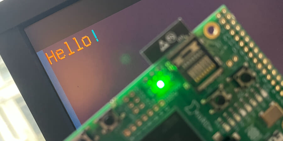
If you run the ch05 demo as is, you'll see the message "Hello!" in text mode. This chapter includes a few simple software examples, all written by hand in bare-metal RISC-V asm:
- hello.s - display "Hello!" using text mode
- framecount.s - hexadecimal frame counter
- jump.s - jumping figure animation
- palette.s - load a palette into clut and display each colour
To change the software loaded at design time, amend FILE_SOFT in your dev board's top_ch05.v. You need to reference the compiled .mem file.
The CPU and memory map aren't in their full form, so I've stuck to simple examples that fit in a few lines of assembler. In the following chapters, we'll develop our software library and tackle more interesting examples when the hardware is nearer its final form.
There's a separate chapter 5 software page that explores the examples in more detail.
Compiling Software
The software examples are available pre-compiled in the Isle repo. If you'd like to compile them yourself or write your own, read the Software Build Guide.
CPU Talking
Each dev board has its own top module, but they all interface with a common chapter 5 design, shown below. The ch05 design includes the CPU, ram, text mode, colour lookup table, and hardware registers, plus it handles two separate clock domains. Not bad for a few hundred lines of Verilog, most of which are interfaces between modules.
module ch05 #(
    parameter BPC=5,            // bits per colour channel
    parameter BG_COLR='h0886,   // background colour (RGB555)
    parameter CORDW=16,         // signed coordinate width (bits)
    parameter DISPLAY_MODE=0,   // display mode (see display_modes.vh)
    parameter FILE_FONT="",     // font glyph ROM file
    parameter FILE_PAL="",      // initial palette for CLUT
    parameter FILE_SOFT="",     // initial software in system ram
    parameter FILE_TXT="",      // initial text file for tram
    parameter FONT_COUNT=128,   // number of glyphs in font ROM
    parameter GLYPH_HEIGHT=16,  // font glyph height (pixels)
    parameter GLYPH_WIDTH=8     // font half-width glyph width (pixels)
    ) (
    input  wire clk_sys,                    // system clock
    input  wire clk_pix,                    // pixel clock (used by display)
    input  wire rst_sys,                    // reset (system clock domain)
    input  wire rst_pix,                    // reset (pixel clock domain)
    output reg  signed [CORDW-1:0] disp_x,  // horizontal display position
    output reg  signed [CORDW-1:0] disp_y,  // vertical display position
    output reg  disp_hsync,                 // horizontal display sync
    output reg  disp_vsync,                 // vertical display sync
    output reg  disp_de,                    // display data enable
    output reg  disp_frame,                 // high for one cycle at frame start
    output reg  [BPC-1:0] disp_r,           // red display channel
    output reg  [BPC-1:0] disp_g,           // green display channel
    output reg  [BPC-1:0] disp_b            // blue display channel
    );

    `include "display_modes.vh"

    // CPU, bus, sysram
    localparam CPU_RESET_ADDR = 'h8000;  // must match linker script
    localparam BUSW = 14;  // bus address width (words) - 2^14 × 4 bytes = 64K
    localparam SYSRAM_ADDRW = 12;  // sysram word width - 2^12 words = 16K

    // text mode
    localparam TEXT_CIDXW =  4;  // 16 colours available in textmode
    localparam TRAM_ADDRW = 11;  // tram address width (bits)
    localparam TRAM_HRES  = 84;  // tram width (chars) - 84x8 = 672
    localparam TRAM_VRES  = 24;  // tram height (chars) - 24x16 = 384
    localparam [TRAM_ADDRW-1:0] TRAM_DEPTH = TRAM_HRES * TRAM_VRES;
    localparam TRAM_LAT   =  2;  // tram read latency (cycles; min=1, max=2)

    // internal system params
    localparam WORD = 32;  // machine word size (bits)
    localparam BYTE =  8;  // machine byte size (bits)
    localparam BYTE_CNT = WORD / BYTE;  // bytes in word (for write enable)
    localparam CIDX_ADDRW = 8;   // colour index address width 2^8 = 256 colours
    localparam COLRW = 3 * BPC;  // colour width across three channels (bits)
    localparam CLUT_LAT =   2;   // clut display read latency (cycles; min=1)

    // display signals
    wire signed [CORDW-1:0] dx, dy;
    wire hsync, vsync, de;
    wire frame_start;
    wire frame_start_sys;  // frame start in system clock domain

    // CPU signals
    wire [WORD-1:0] cpu_addr;  // external address is always word width
    wire [WORD-1:0] cpu_wdata;
    wire [BYTE_CNT-1:0] cpu_wmask;
    wire [WORD-1:0] cpu_rdata;
    wire cpu_rstrb;
    wire cpu_rbusy;
    wire cpu_wbusy;


    //
    // RISC-V CPU
    //

    FemtoRV32 #(
        .ADDRW(BUSW+2),  // +2 for byte addressing
        .RESET_ADDR(CPU_RESET_ADDR)
    ) cpu (
        .clk(clk_sys),
        .rst_n(!rst_sys),
        .mem_addr(cpu_addr),
        .mem_wdata(cpu_wdata),
        .mem_wmask(cpu_wmask),
        .mem_rdata(cpu_rdata),
        .mem_rstrb(cpu_rstrb),
        .mem_rbusy(cpu_rbusy),
        .mem_wbusy(cpu_wbusy),
        .irq(1'b0)  // no interrupts
    );


    //
    // Bus
    //

    wire [BUSW-1:0] io_addr = cpu_addr[BUSW+1:2];  // IO bus is word addressed
    wire [BYTE_CNT-1:0] io_wstrb = cpu_wmask;
    wire [WORD-1:0] io_wdata = cpu_wdata;
    wire io_rstrb = cpu_rstrb;

    // address decoding for chip select signals
    wire sysram_cs = (io_addr[BUSW-1:BUSW-2] == 'b10);
    wire tram_cs   = (io_addr[BUSW-1:BUSW-2] == 'b01);
    wire clut_cs   = (io_addr[BUSW-1:BUSW-2] == 'b00);
    wire hwreg_cs  = (io_addr[BUSW-1:BUSW-2] == 'b11);

    // CPU IO busy - not required in this design
    assign cpu_wbusy = 0;
    assign cpu_rbusy = 0;

    // read data
    reg  [WORD-1:0] io_rdata;
    wire [WORD-1:0] sysram_dout;
    wire [WORD-1:0] tram_dout_sys;
    wire [COLRW-1:0] clut_dout_sys;
    reg  [WORD-1:0] hwreg_dout;  // reg as not separate module
    always @(*) begin
        case(1'b1)
            sysram_cs: io_rdata = sysram_dout;
            tram_cs:   io_rdata = tram_dout_sys;
            clut_cs:   io_rdata = {{WORD-COLRW{1'b0}}, clut_dout_sys};
            hwreg_cs:  io_rdata = hwreg_dout;
            default:   io_rdata = 0;
        endcase
    end
    assign cpu_rdata = io_rdata;


    //
    // System RAM (sysram)
    //

    sysram #(
        .BYTE(BYTE),
        .BYTE_CNT(BYTE_CNT),
        .WORD(WORD),
        .ADDRW(SYSRAM_ADDRW),
        .FILE_SOFT(FILE_SOFT)
    ) sysram_inst (
        .clk(clk_sys),
        .we(io_wstrb & {BYTE_CNT{sysram_cs}}),
        .re(io_rstrb & sysram_cs),
        .addr(io_addr[SYSRAM_ADDRW-1:0]),
        .din(io_wdata),
        .dout(sysram_dout)
    );


    //
    // Text Mode RAM (tram)
    //

    wire [TRAM_ADDRW-1:0] tram_addr_disp;
    wire [WORD-1:0] tram_dout_disp;

    tram #(
        .BYTE(BYTE),
        .BYTE_CNT(BYTE_CNT),
        .WORD(WORD),
        .ADDRW(TRAM_ADDRW),
        .FILE_TXT(FILE_TXT)
    ) tram_inst (
        .clk_sys(clk_sys),
        .clk_pix(clk_pix),
        .we_sys(io_wstrb & {BYTE_CNT{tram_cs}}),
        .re_sys(io_rstrb & tram_cs),
        .addr_sys(io_addr[TRAM_ADDRW-1:0]),
        .din_sys(io_wdata),
        .dout_sys(tram_dout_sys),
        .addr_disp(tram_addr_disp),
        .dout_disp(tram_dout_disp)
    );


    //
    // Text Mode
    //

    // fixed tram size for now; CPU will control through hardware registers
    reg signed [TRAM_ADDRW-1:0] text_hres = TRAM_HRES;
    reg signed [TRAM_ADDRW-1:0] text_vres = TRAM_VRES;

    reg [TRAM_ADDRW-1:0] scroll_offs = 0*84;  // scroll text display (use lines of chars)
    wire [TEXT_CIDXW-1:0] text_pix;
    wire text_paint;  // signals when to enable text painting

    textmode #(
        .CORDW(CORDW),
        .WORD(WORD),
        .ADDRW(TRAM_ADDRW),
        .CIDXW(TEXT_CIDXW),
        .CLUT_LAT(CLUT_LAT),
        .FILE_FONT(FILE_FONT),
        .FONT_COUNT(FONT_COUNT),
        .GLYPH_HEIGHT(GLYPH_HEIGHT),
        .GLYPH_WIDTH(GLYPH_WIDTH),
        .TRAM_DEPTH(TRAM_DEPTH),
        .TRAM_LAT(TRAM_LAT)
    ) textmode_inst (
        .clk_pix(clk_pix),
        .rst_pix(rst_pix),
        .frame_start(frame_start),
        .dx(dx),
        .dy(dy),
        .scroll_offs(scroll_offs),
        .text_hres(text_hres),
        .text_vres(text_vres),
        .win_start(WIN_START_CORD),
        .win_end(WIN_END_CORD),
        .scale(DISPLAY_SCALE),
        .tram_data(tram_dout_disp),
        .tram_addr(tram_addr_disp),
        .pix(text_pix),
        .paint(text_paint)
    );


    //
    // CLUT
    //

    wire [CIDX_ADDRW-1:0] clut_addr_disp;
    wire [COLRW-1:0] clut_dout_disp;

    clut #(
        .ADDRW(CIDX_ADDRW),
        .DATAW(COLRW),
        .FILE_PAL(FILE_PAL)
    ) clut_inst (
        .clk_sys(clk_sys),
        .clk_pix(clk_pix),
        .we_sys(&io_wstrb & clut_cs),  // word write only (reduction AND)
        .re_sys(io_rstrb & clut_cs),
        .addr_sys(io_addr[CIDX_ADDRW-1:0]),
        .din_sys(io_wdata[COLRW-1:0]),
        .dout_sys(clut_dout_sys),
        .addr_disp(clut_addr_disp),
        .dout_disp(clut_dout_disp)
    );


    //
    // Hardware Registers
    //

    // must match software
    localparam [BUSW-1:0] FRAME_FLAG = 'hC110 >> 2;  // word addressing
    localparam [BUSW-1:0] FRAME_FLAG_CLR = 'hC114 >> 2;

    // frame flag
    reg frame_flag, frame_flag_clr;

    // clear frame flag (strobe)
    always @(*) frame_flag_clr = (&io_wstrb && (io_addr == FRAME_FLAG_CLR));

    // update frame flag
    always @(posedge clk_sys) begin
        if (frame_start_sys) frame_flag <= 1;
        else if (frame_flag_clr) frame_flag <= 0;
        if (rst_sys) frame_flag <= 0;
    end

    always @(posedge clk_sys) begin
        if (io_rstrb & hwreg_cs) begin  // read hardware register
            if (io_addr == FRAME_FLAG) hwreg_dout <= {{WORD-1{1'b0}}, frame_flag};
        end
        if (rst_sys) hwreg_dout <= 0;
    end


    //
    // Display Sync Signals and Coordinates
    //

    display_sync_gen #(
        .CORDW(CORDW),
        .DISPLAY_MODE(DISPLAY_MODE)
    ) display_sync_gen_inst (
        .clk_pix(clk_pix),
        .rst_pix(rst_pix),
        .dx(dx),
        .dy(dy),
        .hsync(hsync),
        .vsync(vsync),
        .de(de),
        .frame_start(frame_start),
        .line_start()
    );

    xd xd_frame_start (
        .clk_src(clk_pix),
        .clk_dst(clk_sys),
        .flag_src(frame_start),
        .flag_dst(frame_start_sys)
    );


    //
    // Painting & Display Output
    //

    assign clut_addr_disp = {{CIDX_ADDRW-TEXT_CIDXW{1'b0}}, text_pix};

    // delay background visibility for clut latency
    wire [CLUT_LAT-1:0] bg_visible = {{(CLUT_LAT-1){1'b0}}, ~text_paint};
    reg  [CLUT_LAT-1:0] bg_visible_pipe;
    always @(posedge clk_pix) bg_visible_pipe <= (bg_visible_pipe << 1) | bg_visible;

    // paint colours
    reg [BPC-1:0] paint_r, paint_g, paint_b;
    always @(*) {paint_r, paint_g, paint_b} = bg_visible_pipe[CLUT_LAT-1] ? BG_COLR : clut_dout_disp;

    // register display signals
    always @(posedge clk_pix) begin
        disp_x <= dx;
        disp_y <= dy;
        disp_hsync <= hsync;
        disp_vsync <= vsync;
        disp_de <= de;
        disp_frame <= frame_start;
        disp_r <= (de) ? paint_r : 'h0;  // paint colour but black in blanking
        disp_g <= (de) ? paint_g : 'h0;
        disp_b <= (de) ? paint_b : 'h0;
    end
endmodule
System RAM
A CPU needs ram to hold code and data. To distinguish the main ram used by the CPU from other types of memory (such as video ram), we refer to it as System RAM (sysram). In this chapter, we limit ourselves to 16 KiB of sysram using FPGA block ram (bram). Bram requires a trivial Verilog module and provides predictable low latency. Naturally, there's a downside. Bram limits us to very small memories, while our dev boards have positively bountiful sdram. We'll look at sdram in a later chapter.
Addressing Memory
Before we look at our memory module, we need to consider the dry but important topic of addressing. Byte addressing is the norm for all general-purpose CPUs. With byte addressing, you can access an individual byte in memory even with a 32 or 64-bit CPU.
We're so used to thinking of data sizes in bytes that we rarely stop to think about it, but there's no fundamental reason we should divide data into 8-bit chunks. If a CPU is 32-bit, why not address memory in units of 32-bit words? Word addressing would be simpler, and a 32-bit CPU could access 16 GiB of memory vs 4 GiB with byte addressing.
However, the dominant UTF-8 text encoding is byte-based and with good reason. CPU performance depends on cache hits, so efficient storage of frequently used data, such as text, is essential.
32-bit RISC-V includes separate instructions for loading (reading) and storing (writing) words (32 bit), half words (16 bit), and bytes (8 bit), but the memory interface is 32 bits wide. For loads, the CPU receives a word, but chooses the correct byte or half word as appropriate. For stores, the CPU tells us which bytes to write from the 32-bit word using a 4-bit write mask.
A simple, efficient hardware approach is word addressing with byte write mask and naturally aligned data. With naturally aligned data, the address must be a multiple of the data width; for example, you can read a word from address 16 or 20 (both divisible by 4) but not from address 17.
Memory Interface
Our chosen RISC-V CPU has a simple native memory interface:
output [31:0] mem_addroutput [31:0] mem_wdataoutput [3:0] mem_wmaskinput [31:0] mem_rdataoutput mem_rstrb
There are also busy signals, but we'll hold off considering them until the next chapter.
If we can respond correctly to these read and write signals, we can interface with the CPU.
To read (load) data from memory, the CPU puts the address in mem_addr and sets mem_rstrb (read strobe) to high. The following clock cycle the CPU reads the data from mem_rdata.
To write (store) data to memory, the CPU puts the address in mem_addr, the data in mem_wdata, and sets the bits of mem_wmask (write mask). The CPU is 32-bit but can address individual bytes; the write mask determines whether a full word, half word, or individual byte is written.
mem_addr is a byte address, but we only care about the word address, so we discard the two lower bits:
wire [BUSW-1:0] io_addr = cpu_addr[BUSW+1:2];We use io_addr to interface with our hardware, including sysram.
Sysram Module
Now that we understand the memory interface and addressing, we can create our sysram.v (doc) module:
module sysram #(
    parameter ADDRW=12,      // address width (bits)
    parameter BYTE=8,        // machine byte size (bits)
    parameter BYTE_CNT=4,    // bytes in machine word
    parameter FILE_SOFT="",  // optional initial software to load
    parameter WORD=32        // machine word size (bits)
    ) (
    input  wire clk,                // clock
    input  wire [BYTE_CNT-1:0] we,  // write enable
    input  wire re,                 // read enable
    input  wire [ADDRW-1:0] addr,   // address
    input  wire [WORD-1:0] din,     // data in
    output reg  [WORD-1:0] dout     // data out
    );

    localparam DEPTH=2**ADDRW;

    reg [WORD-1:0] sysram_mem [0:DEPTH-1];

    initial begin
        if (FILE_SOFT != "") begin
            $display("Load software file '%s' into sysram.", FILE_SOFT);
            $readmemh(FILE_SOFT, sysram_mem);
        end
    end

    // system port (read-write)
    integer i;
    always @(posedge clk) begin
        if (re) dout <= sysram_mem[addr];
        for (i=0; i<BYTE_CNT; i=i+1) begin
            if (we[i]) sysram_mem[addr][i*BYTE +: BYTE] <= din[i*BYTE +: BYTE];
        end
    end
endmodule
This module provides everything we need to interface with the CPU. When we get a read enable signal (re), we return the word at addr (word address). If the CPU only needs a byte or a half word, it ignores the bits it doesn't need. When write enable (we) is non-zero, the memory stores data to addr, writing a byte for each bit in we.
The optional FILE_SOFT parameter lets us load software at design time. The for loop saves us from writing out the logic for each of the four bytes, but all writes are written simultaneously in one clock cycle.
MMIO
If we were content with just a CPU and system ram, we could wire the CPU directly to sysram and our job would be done. But with only sysram we'd have a very boring computer, without any display, audio, or input capabilities. Using memory-mapped IO (MMIO), we can connect multiple hardware devices to the CPU and access them in the same way as sysram, but at different addresses.
64 KiB memory map for chapter 5 (addresses in hexadecimal):
- 0x0000 - clut (to 0x00FF - 256B)
- 0x4000 - tram (to 0x5FFF - 8K)
- 0x8000 - sysram (to 0xBFFF - 16K)
- 0xC000 - hardware registers
The clut is the colour lookup table (introduced in Chapter 2 - Bitmap Grapics), and tram is the text mode ram (see Chapter 4 - Text Mode). We'll discuss hardware registers shortly. Later, we'll introduce a 24-bit memory map with support for larger memories and more devices.
When the CPU reads/writes data, it needs to be routed from/to the correct device. In our simple memory map, the first two bits of the address are unique for each of the four memory areas. The logic in ch05.v takes advantage of this to create the chip select signals:
// address decoding for chip select signals
wire sysram_cs = (io_addr[BUSW-1:BUSW-2] == 'b10);
wire tram_cs   = (io_addr[BUSW-1:BUSW-2] == 'b01);
wire clut_cs   = (io_addr[BUSW-1:BUSW-2] == 'b00);
wire hwreg_cs  = (io_addr[BUSW-1:BUSW-2] == 'b11);
With the chip select signals, we can route reads and writes to the correct device, for sysram:
.we(io_wstrb & {BYTE_CNT{sysram_cs}}),
.re(io_rstrb & sysram_cs),
Because write-enable is 4 bits wide, we duplicate chip select to 4 bits before performing the bitwise AND.
The read and write enable signals are similar for the other devices.
Finally, we need a read mux to select the correct subsystem based on the address. We represent a mux using a case statement:
always @(*) begin
    case(1'b1)
        sysram_cs: io_rdata = sysram_dout;
        tram_cs:   io_rdata = tram_dout_sys;
        clut_cs:   io_rdata = {{WORD-COLRW{1'b0}}, clut_dout_sys};
        hwreg_cs:  io_rdata = hwreg_dout;
        default:   io_rdata = 0;
    endcase
end
ProTip: The clut data, clut_dout_sys, is narrower than a word, so we zero extend it to 32 bits.
Hardware Registers
The tram and clut work much like the sysram, and we read and write from them in the normal way, but we also have hardware registers. A hardware register provides an interface to our hardware, a way to configure and control it. In this chapter, we have two registers:
FRAME_FLAG(0xC110) - set to 1 at the start of each frame (read-only)FRAME_FLAG_CLR(0xC114) - writing to this register sets FRAME_FLAG to 0 (strobe)
With the frame flag, we can perform actions every display frame, e.g. for animation. Because this isn't an interrupt, we can't raise the frame flag for one cycle and expect the CPU to notice. Instead, the flag remains raised until the CPU writes to FRAME_FLAG_CLR to clear it. FRAME_FLAG_CLR is a strobe register; the value written doesn't matter, just that a write occurs to the correct address.
For example, the frame_waitn function waits for the start of N frames before returning:
frame_waitn:
    beqz a0, 1f  # don't wait if 'a0' is zero
    li   t6, HWREG_BASE  # hwreg base addr
0:
    lw   t0, FRAME_FLAG(t6)  # load frame flag
    beqz t0, 0b  # loop if flag not set
    sw   zero, FRAME_FLAG_CLR(t6)  # clear frame flag (strobe)

    addi a0, a0, -1  # decrement remaining frame count
    bnez a0, 0b  # loop if frames remain
1:
    ret
You can see this function in action in the Chapter 5 Software.
In future chapters, we'll introduce additional hardware registers for text mode, 2D drawing, keyboard, etc.
With that brief introduction to interfacing our CPU to our hardware, we're ready to add more hardware and software to our computer, starting with keyboard input.
Input
Our computer can communicate with us via the display, but it has no input. Our next chapter, Input Output, tackles input via UART, and we'll begin work on a software library, which makes text output simple with our text mode.
Next step: Chapter 6 - Input Output, Chapter 5 Software, or Isle Index
Further Reading
- RISC-V Assembler Guide by Will Green
- From Blinker to RISC-V - FemtoRV tutorial by Bruno Levy
- RISC-V Technical Specifications (riscv.org)