Hello Nexys - Part 1
This two-part tutorial provides a quick introduction to FPGA development with SystemVerilog and the Digilent Nexys Video board. No prior experience of FPGA development is required, but basic knowledge of programming concepts is assumed. If you can write a simple program with Python or JavaScript, you shouldn’t have any trouble.
I find working with FPGAs gives me a sense of delight so often lacking in modern software development. There’s something profoundly satisfying about designing at the hardware level, be it drawing graphics on a screen, producing sound from a speaker, or even implementing your own CPU from scratch. I hope you find this tutorial helpful and have fun with FPGAs. This series is also available for the Arty.
Already completed part 1? Jump to part 2.
Requirements
For this series, we are be using the Digilent Nexys Video, a $480 dev board based on a Xilinx Artix-7 FPGA. This board is widely available and supports Xilinx’s latest Vivado software, which runs on Linux and Windows.
For this Hello Nexys series you need:
- Digilent Nexys Video
- Micro USB cable to program the Nexys Video board
- 12V power adaptor (EU/US plug is provided by Digilent - UK users will need an adaptor)
- Xilinx Vivado 2019 or later: Download and Install Guide
- Digilent board files
Source
The SystemVerilog designs featured in this series are available from the projf-explore git repo under the open-source MIT licence: build on them to your heart’s content. The rest of the blog content is subject to standard copyright restrictions: don’t republish it without permission.
Hello World with SystemVerilog & Vivado
We’re going to start with the traditional dev board “hello, world”: using simple logic to control the green LEDs on our board. In part 2 we move onto clocks, counting, and pulse width modulation.
Terminology
Before we dive into creating our first project, I should explain a couple of terms:
- SystemVerilog is a hardware description language (HDL) that allows you to express your design at a (reasonably) high level instead of directly describing logic gates (AND, OR, NOT). This is roughly analogous to how C lets you express your software design at a higher level than assembly language. Other HDLs include VHDL, SpinalHDL, and nMigen.
- Vivado is the FPGA development suite from Xilinx. It includes everything you need to write SystemVerilog and program a Xilinx FPGA. There’s no getting around the fact it’s a monster, requiring around 20 GiB of disk space. Thankfully it has a no-cost version and is reasonably intuitive once you’ve played with it for a little while. Vivado is available for Windows and Linux (Ubuntu RHEL/CentOS, & SUSE), but not for macOS.
The Nexys Video Board

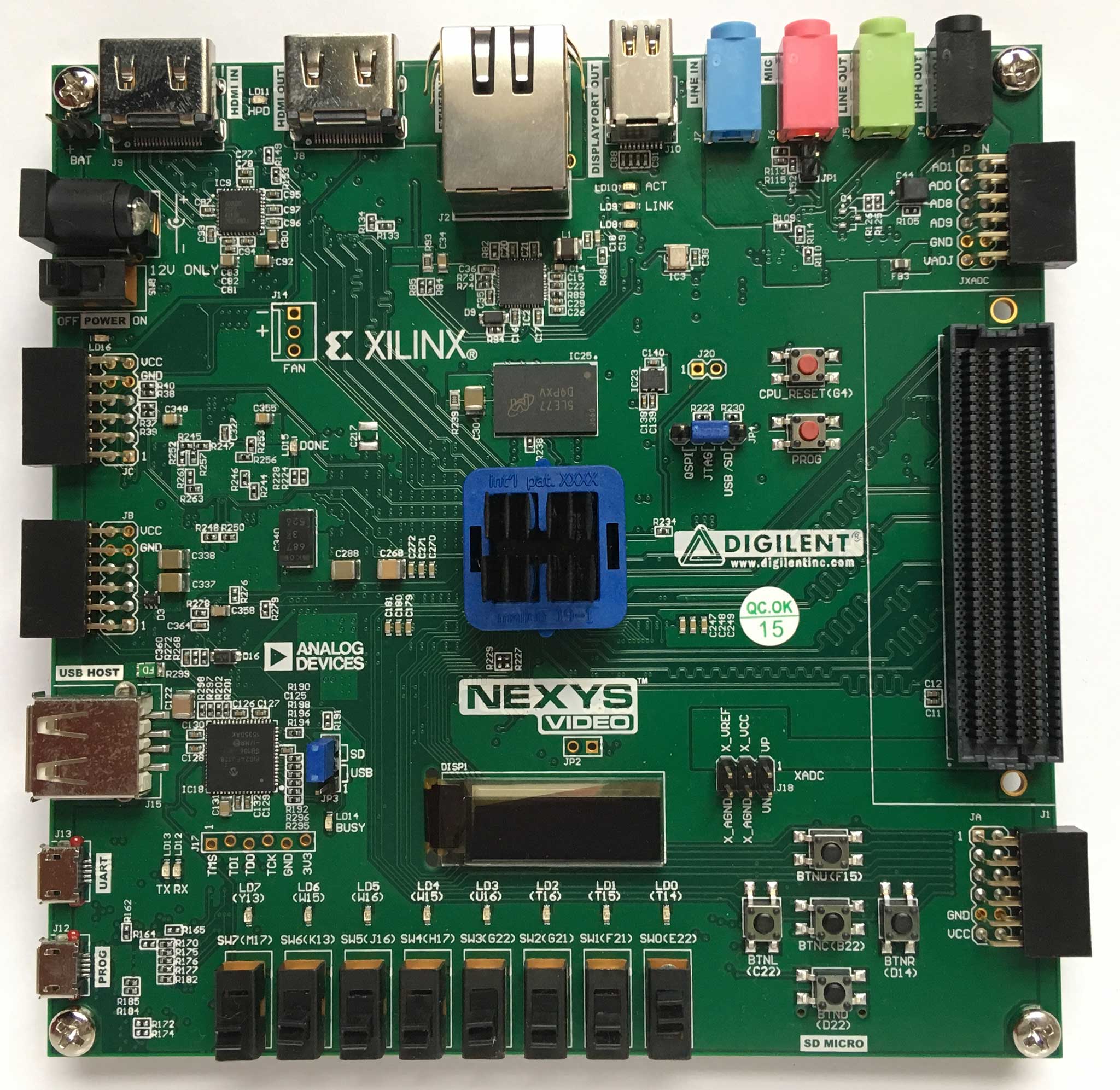
In this part, we’re interested in the eight green LEDs (LD0-7), eight slide switches (SW0-7), and five push buttons (BTNx). You can see these towards the bottom of the board in the above photo. The FPGA itself is the square chip in the middle of the board under the heat sink.
Hello World Project
For our first SystemVerilog, we’re going to use a switch to turn an LED off and on. We then extend this to cover multiple LEDs, switches, and buttons.
Creating a Project
- Start Vivado.
- Select “Create Project” under “Quick Start”.
- Project name:
hello-nexys-1and make sure “Create project subdirectory” is selected. - Project Type: “RTL Project” and make sure “Do not specify sources at this time” is selected.
- Default Part: Select “Boards” then choose “Nexys Video”.
If it’s not on the list, you need to quit Vivado and install the board files. - Review the “New Project Summary” and hit “Finish”.
Hello SystemVerilog
- In the top left of the Vivado window, under “Project Manager”, select “Add Sources”.
- Choose “Add or create design sources” and click “Next”.
- Select “Create File” in the middle of the dialog.
- Make sure File type is set to “SystemVerilog” and name the file
top.svthen click “Finish”. - In the “Define Module” dialog hit “OK” then click “Yes” when prompted.
Replace the contents of the top module in top.sv with [src]:
module top (
    input wire logic sw,
    output     logic led
    );

    always_comb begin
        led = sw;
    end
endmodule
The first part of the module defines our inputs and outputs:
sw- one of the four slide switches (labelledSW0on the PCB)led- one of the green LEDs (labelledLD0on the PCB)
The second part of the module is where we write our logic. In this case, we wire up led to sw: when the switch is on the LED is on, when the switch is off the LED is off. Don’t worry about the meaning of always_comb for now; we’ll come back to that in part 2.
Save your file by hitting Ctrl-S or by using the save button at the top left of the editor window (yes, it still looks like a floppy disk).
ProTip: You can use Ctrl+/ to (un)comment the current line in the Vivado editor window.
Direct Connection
You wouldn’t normally directly connect a switch to an LED like this. However, it’s good to be able to work with real hardware right away, so we’ve taken some liberties. In part 2 we’ll store the LED state in a flip-flop.
Constraints File
An FPGA is very flexible; you can connect many different types of inputs and outputs to the many hundreds of pins. Before synthesising our code, we need to tell Vivado how our Nexys board is wired up. Vivado uses constraints to map an input or output, such as led, to the appropriate pin.
- In the top left of the Vivado window, select “Add Sources” under “Project Manager”.
- Choose “Add or create constraints” and click “Next”.
- Select “Create File” in the middle of the dialog.
- Make sure File type is set to “XDC” and name the file
nexys.xdcthen click “Finish”.
Select nexys.xdc in the editor window, add the following [src] content then save the file.
## FPGA Configuration I/O Options
set_property CONFIG_VOLTAGE 3.3 [current_design]
set_property CFGBVS VCCO [current_design]

# I/O Pins
set_property -dict {PACKAGE_PIN E22 IOSTANDARD LVCMOS12} [get_ports {sw}];
set_property -dict {PACKAGE_PIN T14 IOSTANDARD LVCMOS25} [get_ports {led}];
ProTip: These constraints are written in Tcl, which is used throughout Vivado.
Design to Board
To bring our design to life on the Nexys board, we need to go through four steps:
- Synthesis - convert the SystemVerilog into logic gates
- Implementation - optimise and lay out the logic for the target FPGA
- Generate Bitstream - generate the FPGA bitstream file from the implementation
- Program Device - load the bitstream into the FPGA
Even on a fast PC, this whole process can take a few minutes, so be patient.
- Click the green play button at the top of the Vivado screen.
- Select “Run Synthesis”.
If a “Launch Runs” dialog appears then just select “OK”.
You’ll see a message “Running synth_design” at the top-right of Vivado. - A dialog appears prompting you to “Run Implementation”.
Click “OK” to start implementation. - A dialog appears saying “Implementation successfully completed”.
Select “Generate Bitstream” and click “OK”. - A dialog appears saying “Bitstream Generation successfully completed”.
Select “Open Hardware Manager” and click “OK”.
If you accidentally close any step you can find commands to run the different stages on the left-hand side of the Vivado window.
Hardware Manager
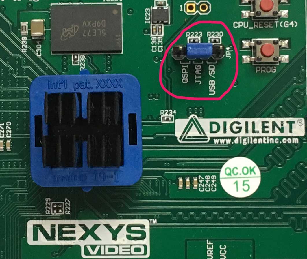
- Ensure Nexys jumper JP4 is in the middle position for JTAG programming (see photo, below).
- Connect your Nexys board to your PC using a micro USB cable.
- At the bottom left of Vivado select “Open Target” under “Open Hardware Manager”.
- Choose “Auto Connect” from the menu. If this fails, try again, it can be temperamental.
- Select “Program Device” under “Open Hardware Manager”.
- There should be one option “xc7a200t_0”; this is your Nexys board.
- Browse to your bitstream file
hello-nexys-1/hello-nexys-1.runs/impl_1/top.bit. - Click “Program”.
If you’re on Linux and hardware manager never connects then you may have forgotten to install the cable drivers.

Hello LED
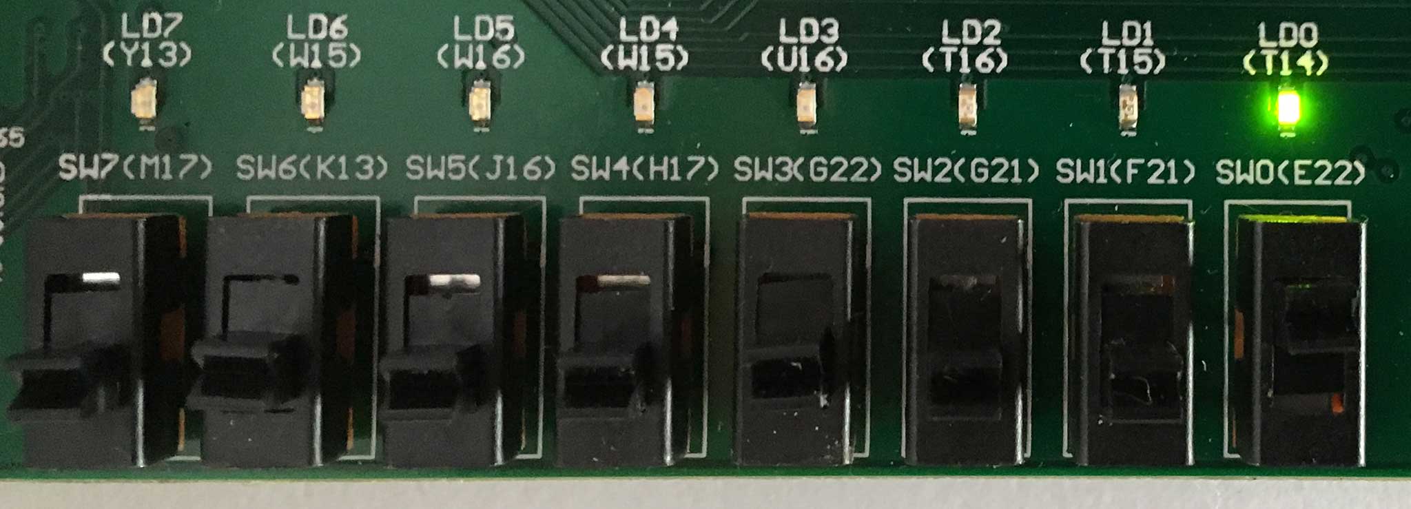
Slide the switch SW0 on and off on your board to control green LED LD0.

This functionality isn’t anything you couldn’t trivially achieve with a microcontroller. However, it’s worth pausing to think about what you’ve done here. You’ve created a simple circuit board within the FPGA. There is no CPU running code here: it’s as if you’d wired up the switch to the LED on a breadboard.
Moar Switches, Moar LEDs!
You didn’t buy an FPGA to emulate a single wire on a breadboard; let’s extend our design so that one switch can control two LEDs. Granted you didn’t buy an FPGA board to do that either, but it does at least involve some logic!
If you’re still in Hardware Manager; you can get back to your Verilog source code by selecting “Project Manager” at the top left of the Vivado window.
Replace the existing top module in top.sv with the following [src]:
module top (
    input wire logic [1:0] sw,
    output     logic [3:0] led
    );

    always_comb begin
        if (sw[0]) begin
            led[1:0] = 2'b11;
        end else begin
            led[1:0] = 2'b00;
        end

        if (sw[1]) begin
            led[3:2] = 2'b11;
        end else begin
            led[3:2] = 2'b00;
        end
    end
endmodule
2'b defines a 2-bit binary literal: we have two LEDs each expecting a signal, so a two-bit value is appropriate here. You use d for decimal literals, and h for hexadecimal literals:
2'b11- 2 bits with value 112 (decimal 3)4'd5- 4 bits with value 58'h5E- 8 bits with value 5E16 (decimal 94)15'h7FF- 15 bits with value 7FF16 (decimal 2,047)
You can also see how we’ve referred to multiple LEDs: led[1:0] includes both led[0] and led[1].
We’re added a switch and three LEDs to our design, but we haven’t defined them in our constraints file; Vivado won’t know what to connect them to. Open up nexys.xdc and replace it with [src]:
## FPGA Configuration I/O Options
set_property CONFIG_VOLTAGE 3.3 [current_design]
set_property CFGBVS VCCO [current_design]

## Slide Switches
set_property -dict {PACKAGE_PIN E22 IOSTANDARD LVCMOS12} [get_ports {sw[0]}];
set_property -dict {PACKAGE_PIN F21 IOSTANDARD LVCMOS12} [get_ports {sw[1]}];

## LEDs
set_property -dict {PACKAGE_PIN T14 IOSTANDARD LVCMOS25} [get_ports {led[0]}];
set_property -dict {PACKAGE_PIN T15 IOSTANDARD LVCMOS25} [get_ports {led[1]}];
set_property -dict {PACKAGE_PIN T16 IOSTANDARD LVCMOS25} [get_ports {led[2]}];
set_property -dict {PACKAGE_PIN U16 IOSTANDARD LVCMOS25} [get_ports {led[3]}];
Rerun synthesis, implementation, bitstream generation, and program the board as before. You should be able to control two LEDs with each of the first two slide switches.
Conditional Love
Those if blocks can get annoying fast, plus bad things happen if you don’t provide a value for all possible outcomes (latches: yuuurgh). Verilog has an answer for this with the every-handy conditional operator condition ? value_if_true : value_if_false;
The easiest way to understand it is to see it in action; replace top.sv with the following [src]:
module top (
    input wire logic [1:0] sw,
    output     logic [3:0] led
    );

    always_comb begin
        led[1:0] = sw[0] ? 2'b11 : 2'b00;
        led[3:2] = sw[1] ? 2'b11 : 2'b00;
    end
endmodule
Go through the usual rigmarole of synthesis, implementation, bitstream generation, and programming your board. It should work as before, but I think you’ll agree the conditional operator makes this design simpler to write and understand.
Smooth Operator
We can expand our conditional expressions with logical operators:
- && - logical AND
- || - logical OR
- ! - logical NOT (or negation)
These work as you’d expect from software development; for example:
A && B is true if both A and B are true.
These logical operators are not to be confused with bitwise operators, such as a single &, which operate on the individual bits of a value. We’ll encounter bitwise operators in later tutorials.
For now let’s test two switches with the logical AND operator and add a push button [src]:
module top (
    input wire logic [3:0] sw,
    input wire logic btnc, btnd, btnl, btnr, btnu,
    output     logic [3:0] led
    );

    always_comb begin
        if (sw[0] == 0 && sw[1] == 1) begin
            led[3:0] = btnc ? 4'b1001 : 4'b0110;
        end else begin
            led[3:0] = 4'b0000;
        end
    end
endmodule
We don’t have push buttons in our constraints; let’s add them and the other slide switches [src]:
## FPGA Configuration I/O Options
set_property CONFIG_VOLTAGE 3.3 [current_design]
set_property CFGBVS VCCO [current_design]

## Slide Switches
set_property -dict {PACKAGE_PIN E22 IOSTANDARD LVCMOS12} [get_ports {sw[0]}];
set_property -dict {PACKAGE_PIN F21 IOSTANDARD LVCMOS12} [get_ports {sw[1]}];
set_property -dict {PACKAGE_PIN G21 IOSTANDARD LVCMOS12} [get_ports {sw[2]}];
set_property -dict {PACKAGE_PIN G22 IOSTANDARD LVCMOS12} [get_ports {sw[3]}];

## Buttons
set_property -dict {PACKAGE_PIN B22 IOSTANDARD LVCMOS12} [get_ports {btnc}];
set_property -dict {PACKAGE_PIN D22 IOSTANDARD LVCMOS12} [get_ports {btnd}];
set_property -dict {PACKAGE_PIN C22 IOSTANDARD LVCMOS12} [get_ports {btnl}];
set_property -dict {PACKAGE_PIN D14 IOSTANDARD LVCMOS12} [get_ports {btnr}];
set_property -dict {PACKAGE_PIN F15 IOSTANDARD LVCMOS12} [get_ports {btnu}];

## LEDs
set_property -dict {PACKAGE_PIN T14 IOSTANDARD LVCMOS25} [get_ports {led[0]}];
set_property -dict {PACKAGE_PIN T15 IOSTANDARD LVCMOS25} [get_ports {led[1]}];
set_property -dict {PACKAGE_PIN T16 IOSTANDARD LVCMOS25} [get_ports {led[2]}];
set_property -dict {PACKAGE_PIN U16 IOSTANDARD LVCMOS25} [get_ports {led[3]}];
Rerun synthesis, implementation, bitstream generation, and program your board as before.
SW0 and SW1 control whether the LEDs are enabled; BTNC (centre) selects two different patterns of lights.
Explore
You should put your new skills to use! Create with your own designs using switches, buttons, and LEDs. Just remember that when assigning things they should be the same width; for example, three bits for three LEDs: led[3:1] = 3'b101;
Try answering the following questions:
- How would you test if either the up or down button were pressed?
- What’s wrong with the literal
4'd20? How could you write it? - How is a slide switch different from a push button?
What’s Next?
In part 2 of Hello Nexys, we move onto clocks, counting, and pulse width modulation. You can also check out my recommended FPGA sites.